Memory chiplet
Miden VM supports linear read-write random access memory. This memory is element-addressable, meaning that a single value is located at each address, although reading and writing values to/from memory in batches of four is supported. Each value is a field element in a -bit prime field with modulus . A memory address is a field element in the range .
In this note we describe the rationale for selecting the above design and describe AIR constraints needed to support it.
The design makes extensive use of -bit range checks. An efficient way of implementing such range checks is described here.
Alternative designs
The simplest (and most efficient) alternative to the above design is contiguous write-once memory. To support such memory, we need to allocate just two trace columns as illustrated below.
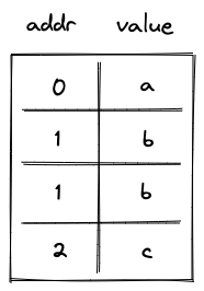
In the above, addr column holds memory address, and value column holds the field element representing the value stored at this address. Notice that some rows in this table are duplicated. This is because we need one row per memory access (either read or write operation). In the example above, value was first stored at memory address , and then read from this address.
The AIR constraints for this design are very simple. First, we need to ensure that values in the addr column either remain the same or are incremented by as we move from one row to the next. This can be achieved with the following constraint:
where is the value in addr column in the current row, and is the value in this column in the next row.
Second, we need to make sure that if the value in the addr column didn't change, the value in the value column also remained the same (i.e., a value stored in a given address can only be set once). This can be achieved with the following constraint:
where is the value in value column at the current row, and is the value in this column in the next row.
As mentioned above, this approach is very efficient: each memory access requires just trace cells.
Read-write memory
Write-once memory is tricky to work with, and many developers may need to climb a steep learning curve before they become comfortable working in this model. Thus, ideally, we'd want to support read-write memory. To do this, we need to introduce additional columns as illustrated below.
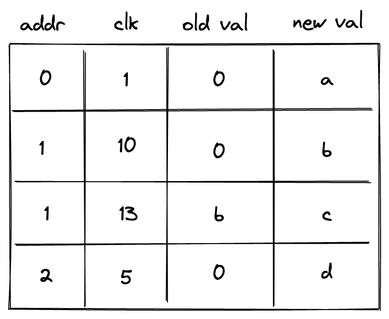
In the above, we added clk column, which keeps track of the clock cycle at which memory access happened. We also need to differentiate between memory reads and writes. To do this, we now use two columns to keep track of the value: old val contains the value stored at the address before the operation, and new val contains the value after the operation. Thus, if old val and new val are the same, it was a read operation. If they are different, it was a write operation.
The AIR constraints needed to support the above structure are as follows.
We still need to make sure memory addresses are contiguous:
Whenever memory address changes, we want to make sure that old val is set to (i.e., our memory is always initialized to ). This can be done with the following constraint:
On the other hand, if memory address doesn't change, we want to make sure that new val in the current row is the same as old val in the next row. This can be done with the following constraint:
Lastly, we need to make sure that for the same address values in clk column are always increasing. One way to do this is to perform a -bit range check on the value of , where is the reference to clk column. However, this would mean that memory operations involving the same address must happen within VM cycles from each other. This limitation would be difficult to enforce statically. To remove this limitation, we need to add two more columns as shown below:
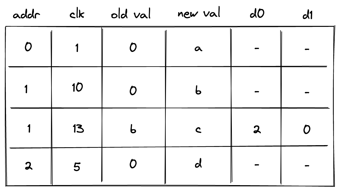
In the above column d0 contains the lower bits of while d1 contains the upper bits. The constraint needed to enforces this is as follows:
Additionally, we need to apply -bit range checks to columns d0 and d1.
Overall, the cost of reading or writing a single element is now trace cells and -bit range-checks.
Non-contiguous memory
Requiring that memory addresses are contiguous may also be a difficult limitation to impose statically. To remove this limitation, we need to introduce one more column as shown below:
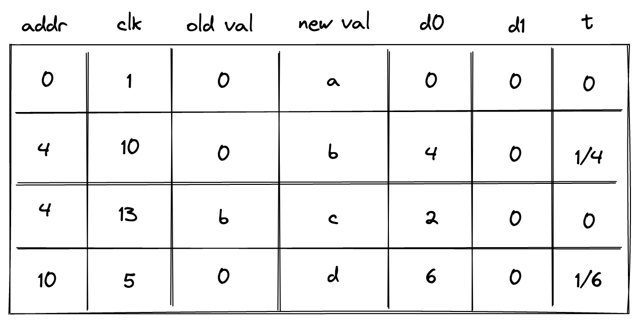
In the above, the prover sets the value in the new column t to when the address doesn't change, and to otherwise. To simplify constraint description, we'll define variable computed as follows:
Then, to make sure the prover sets the value of correctly, we'll impose the following constraints:
The above constraints ensure that whenever the address changes, and otherwise. We can then define the following constraints to make sure values in columns d0 and d1 contain either the delta between addresses or between clock cycles.
| Condition | Constraint | Comments |
|---|---|---|
When the address changes, columns d0 and d1 at the next row should contain the delta between the old and the new address. | ||
When the address remains the same, columns d0 and d1 at the next row should contain the delta between the old and the new clock cycle. |
We can combine the above constraints as follows:
The above constraint, in combination with -bit range checks against columns d0 and d1 ensure that values in addr and clk columns always increase monotonically, and also that column addr may contain duplicates, while values in clk column must be unique for a given address.
Context separation
In many situations it may be desirable to assign memories to different contexts. For example, when making a cross-contract calls, the memories of the caller and the callee should be separate. That is, the caller should not be able to access the memory of the callee and vice-versa.
To accommodate this feature, we need to add one more column as illustrated below.
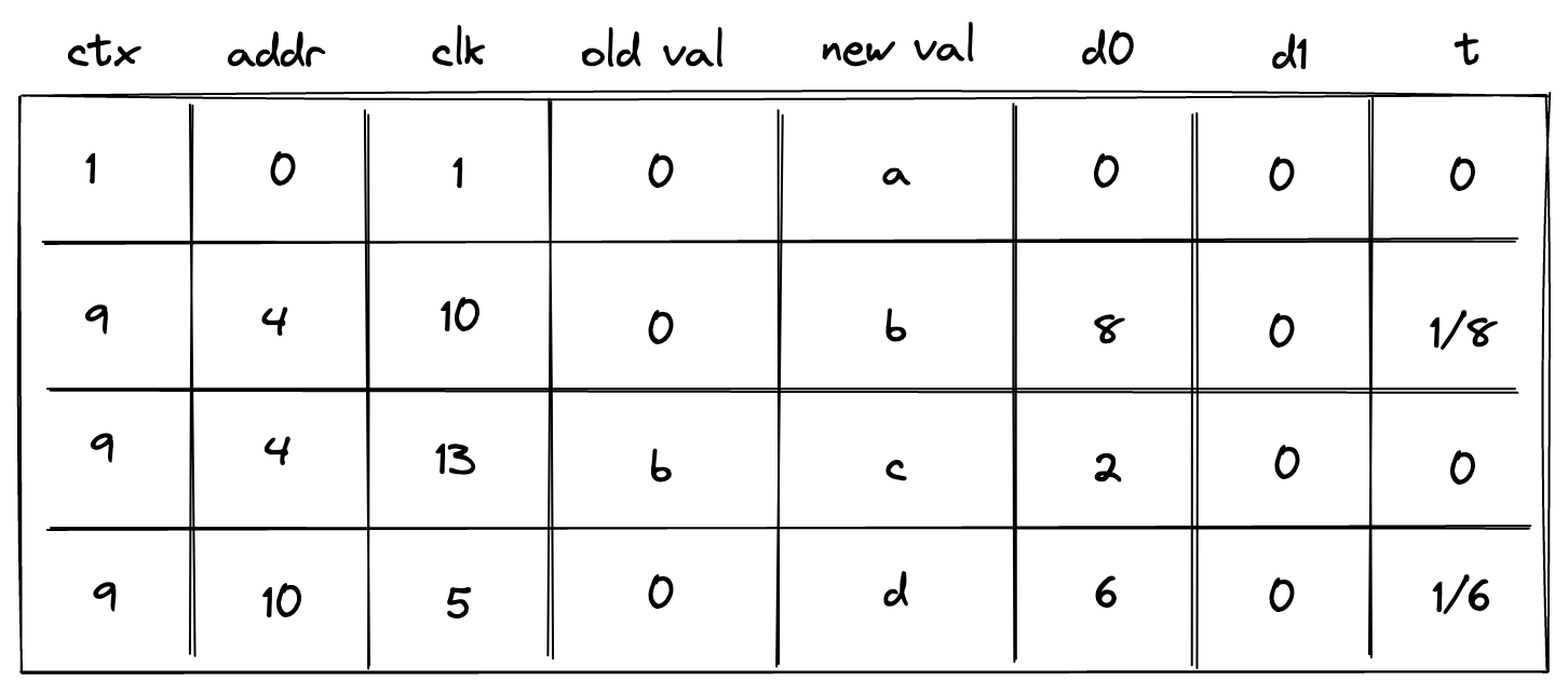
This new column ctx should behave similarly to the address column: values in it should increase monotonically, and there could be breaks between them. We also need to change how the prover populates column t:
- If the context changes,
tshould be set to the inverse , where is a reference to columnctx. - If the context remains the same but the address changes, column
tshould be set to the inverse of . - Otherwise, column
tshould be set to .
To simplify the description of constraints, we'll define two variables and as follows:
Thus, when the context changes, and otherwise. Also, when context remains the same and address changes, and otherwise.
To make sure the prover sets the value of column t correctly, we'll need to impose the following constraints:
We can then define the following constraints to make sure values in columns d0 and d1 contain the delta between contexts, between addresses, or between clock cycles.
| Condition | Constraint | Comments |
|---|---|---|
When the context changes, columns d0 and d1 at the next row should contain the delta between the old and the new contexts. | ||
| | When the context remains the same but the address changes, columns d0 and d1 at the next row should contain the delta between the old and the new addresses. | |
| | When both the context and the address remain the same, columns d0 and d1 at the next row should contain the delta between the old and the new clock cycle. |
We can combine the above constraints as follows:
The above constraint, in combination with -bit range checks against columns d0 and d1 ensure that values in ctx, addr, and clk columns always increase monotonically, and also that columns ctx and addr may contain duplicates, while the values in column clk must be unique for a given combination of ctx and addr.
Notice that the above constraint has degree .
Miden approach
While the approach described above works, it comes at significant cost. Reading or writing a single value requires trace cells and -bit range checks. Assuming a single range check requires roughly trace cells, the total number of trace cells needed grows to . This is about x worse the simple contiguous write-once memory described earlier.
Miden VM frequently needs to deal with batches of field elements, which we call words. For example, the output of Rescue Prime Optimized hash function is a single word. A single 256-bit integer value can be stored as two words (where each element contains one -bit value). Thus, we can optimize for this common use case by making the chiplet handle words as opposed to individual elements. That is, memory is still element-addressable in that each memory address stores a single field element, and memory addresses may be read or written individually. However, the chiplet also handles reading and writing elements in batches of four simultaneously, with the restriction that such batches be word-aligned addresses (i.e. the address is a multiple of 4).
The layout of Miden VM memory table is shown below:
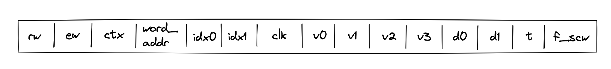
where:
rwis a selector column which is set to for read operations and for write operations.ewis a selector column which is set to when a word is being accessed, and when an element is being accessed.ctxcontains context ID. Values in this column must increase monotonically but there can be gaps between two consecutive values of up to . Also, two consecutive values can be the same.word_addrcontains the memory address of the first element in the word. Values in this column must increase monotonically for a given context but there can be gaps between two consecutive values of up to . Values in this column must be divisible by 4. Also, two consecutive values can be the same.idx0andidx1are selector columns used to identify which element in the word is being accessed. Specifically, the index within the word is computed asidx1 * 2 + idx0.- However, when
ewis set to (indicating that a word is accessed), these columns are meaningless and are set to .
- However, when
clkcontains clock cycle at which the memory operation happened. Values in this column must increase monotonically for a given context and memory word but there can be gaps between two consecutive values of up to .- Unlike the previously described approaches, we allow
clkto be constant in the same context/word address, with the restriction that when this is the case, then only reads are allowed.
- Unlike the previously described approaches, we allow
v0, v1, v2, v3columns contain field elements stored at a given context/word/clock cycle after the memory operation.- Columns
d0andd1contain lower and upper bits of the delta between two consecutive context IDs, addresses, or clock cycles. Specifically:- When the context changes within a frame, these columns contain in the "next" row.
- When the context remains the same but the word address changes within a frame, these columns contain in the "next" row.
- When both the context and the word address remain the same within a frame, these columns contain in the "next" row.
- Column
tcontains the inverse of the delta between two consecutive context IDs, addresses, or clock cycles. Specifically:- When the context changes within a frame, this column contains the inverse of in the "next" row.
- When the context remains the same but the word address changes within a frame, this column contains the inverse of in the "next" row.
- When both the context and the word address remain the same within a frame, this column contains the inverse of in the "next" row.
- Column
f_scwstands for "flag same context and word address", which is set to when the current and previous rows have the same context and word address, and otherwise.
For every memory access operation (i.e., read or write a word or element), a new row is added to the memory table. If neither ctx nor addr have changed, the v columns are set to equal the values from the previous row (except for any element written to). If ctx or addr have changed, then the v columns are initialized to (except for any element written to).
AIR constraints
We first define the memory chiplet selector flags. , and will refer to the chiplet selector flags.
- is set to 1 when the current row is in the memory chiplet.
- is set to 1 when the current row is in the memory chiplet, except for the last row of the chiplet.
- is set to 1 when the next row is the first row of the memory chiplet.
To simplify description of constraints, we'll define two variables and as follows:
Where and .
To make sure the prover sets the value of column t correctly, we'll need to impose the following constraints:
The above constraints guarantee that when context changes, . When context remains the same but word address changes, . And when neither the context nor the word address change, .
We enforce that the rw, ew, idx0 and idx1 contain binary values.
To enforce the values of context ID, word address, and clock cycle grow monotonically as described in the previous section, we define the following constraint.
In addition to this constraint, we also need to make sure that the values in registers and are less than , and this can be done with range checks.
Next, we need to ensure that when the context, word address and clock are constant in a frame, then only read operations are allowed in that clock cycle.
Next, for all frames where the "current" and "next" rows are in the chiplet, we need to ensure that the value of the f_scw column in the "next" row is set to when the context and word address are the same, and otherwise.
Note that this does not constrain the value of f_scw in the first row of the chiplet. This is intended, as the first row's constraints do not depend on the previous row (since the previous row is not part of the same chiplet), and therefore do not depend on f_scw (see "first row" constraints below).
Finally, we need to constrain the v0, v1, v2, v3 columns. We will define a few variables to help in defining the constraints.
The flag is set to when is being accessed, and otherwise. Next, for ,
which is set to when is not written to, and otherwise.
We're now ready to describe the constraints for the v0, v1, v2, v3 columns.
- For the first row of the chiplet (in the "next" position of the frame), for ,
That is, if the next row is the first row of the memory chiplet, and is not written to, then must be .
- For all rows of the chiplet except the first, for ,
That is, if is not written to, then either its value needs to be copied over from the previous row (when ), or it must be set to 0 (when ).
Chiplets bus constraints
Communication between the memory chiplet and the stack is accomplished via the chiplets bus . To respond to memory access requests from the stack, we need to divide the current value in by the value representing a row in the memory table.
Memory row value
This value can be computed as follows:
where
and where is the appropriate operation label of the memory access operation.
To ensure that values of memory table rows are included into the chiplets bus, we impose the following constraint:
On the stack side, for every memory access request, a corresponding value is divided out of the column. Specifics of how this is done are described here.